
2K x 8 Reprogrammable PROM
CY7C291A
CY7C292A/CY7C293A
Cypress Semiconductor Corporation
• 3901 North First Street • San Jose • CA 95134 • 408-943-2600
March 1986 – Revised May 1993
92A
Features
•
Windowed for reprogrammability
•
CMOS for optimum speed/power
•
High speed
—
20 ns (commercial)
—
25 ns (military)
•
Low power
—
660 mW (commercial and military)
•
Low standby power
—
220 mW (commercial and military)
•
EPROM technology 100% programmable
•
Slim 300-mil or standard 600-mil packaging available
•
5V
±
10% V
CC
, commercial and military
•
TTL-compatible I/O
•
Direct replacement for bipolar PROMs
•
Capable of withstanding >2001V static discharge
Functional Description
The CY7C291A, CY7C292A, and CY7C293A are high-perfor-
mance 2K-word by 8-bit CMOS PROMs. They are functionally
identical, but are packaged in 300-mil (7C291A, 7C293A) and
600-mil wide plastic and hermetic DIP packages (7C292A).
The CY7C293A has an automatic power down feature which
reduces the power consumption by over 70% when deselect-
ed. The 300-mil ceramic package may be equipped with an
erasure window; when exposed to UV light the PROM is
erased and can then be reprogrammed. The memory cells uti-
lize proven EPROM floating-gate technology and byte-wide in-
telligent programming algorithms.
The CY7C291A, CY7C292A, and CY7C293A are plug-in re-
placements for bipolar devices and offer the advantages of
lower power, reprogrammability, superior performance and
programming yield. The EPROM cell requires only 12.5V for
the supervoltage and low current requirements allow for gang
programming. The EPROM cells allow for each memory loca-
tion to be tested 100%, as each location is written into, erased,
and repeatedly exercised prior to encapsulation. Each PROM
is also tested for AC performance to guarantee that after cus-
tomer programming the product will meet DC and AC specifi-
cation limits.
A read is accomplished by placing an active LOW signal on
CS
1
, and active HIGH signals on CS
2
and CS
3
. The contents
of the memory location addressed by the address line (A
0
−
A
10
) will become available on the output lines (O
0
−
O
7
).
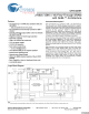
LogicBlock Diagram Pin Configurations
C291A-1
C291A-2
C291A-3
O
7
O
6
O
5
O
4
O
3
O
2
O
1
O
0
PROGRAM-
MABLE
ARRAY
MULTI-
PLEXER
GND
1
2
3
4
5
6
7
8
9
10
11 14
15
16
20
19
18
17
21
24
23
22
A
6
A
5
A
4
A
3
A
2
A
1
A
0
O
0
A
7
O
3
V
CC
A
8
A
9
A
10
O
7
O
6
O
5
O
4
CS
1
O
2
12 13
O
1
CS
3
CS
2
28
4
5
6
7
8
9
10
321 27
1314151617
26
25
24
23
22
21
20
11
12
19
A
5
V
CC
GND
A
6
A
7
O
3
O
1
O
0
18
O
4
O
5
NC
A
0
A
4
A
3
A
10
NC
A
8
A
9
NC
NC
CS
1
CS
2
O
7
O
6
A
2
A
1
CS
3
O
2
CS
1
CS
2
CS
3
POWER
DOWN
7C293A
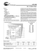
Window available on
7C291A and 7C293A
only.
DIP
LCC/PLCC (Opaque Only)
Top View
Top View
ADDRESS
DECODER
A
0
A
1
A
2
A
3
A
4
A
5
A
6
A
8
A
9
A
10
A
7
COLUMN
ADDRESS
ROW
ADDRESS
7C291A
7C292A
7C293A
7C291A
7C293A


 England
  Deutschland
  France
  Italia
  Polska
  United Kingdom
  Россия
  Nederland
  España
  Magyarország
  Sverige
  România
  Portugal
  Colombia
  Suomi
Suomi  New Zealand
  Česká republika
  Türkiye
  Danmark
  日本
日本